Recent Posts


India operates more than 1800 Global Capability Centers GCCs as of 2026. These centers generate an estimated 65 billion dollars in revenue and employ 2.1 million professionals. A vital component of the Indian IT industry, Global Capability Centers (GCCs) manage engineering design and development projects for parent firms across the world.
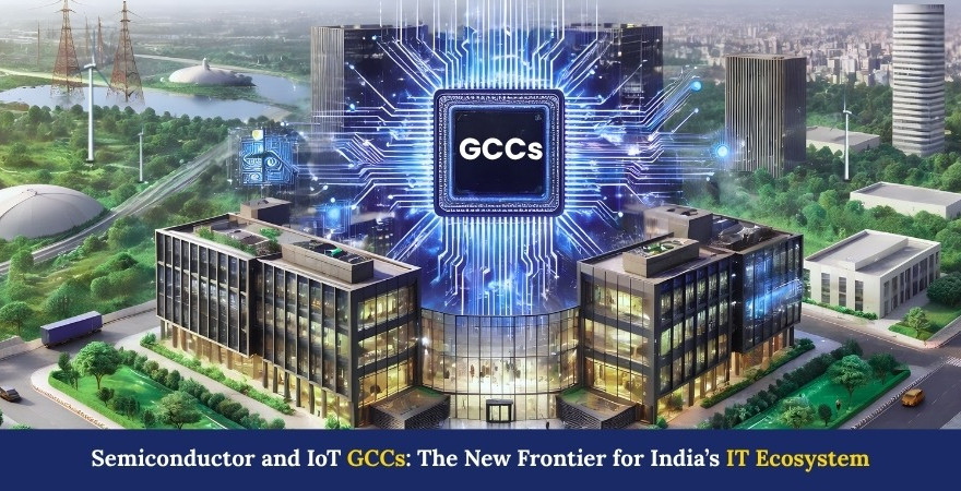
India has long been associated with IT services, supporting multinational corporations via software development, outsourcing, and support functions. This reputation positioned the nation as the “back office of the world.” But the story is changing quickly. India is now more than just a cheap place to get IT services. Thanks to the growth of Global Capability Centers (GCCs), it is becoming a global hub for innovation. These centers, which multinational firms founded, are moving beyond traditional functions and assuming strategic roles in product development, engineering, and research. Semiconductor and Internet of Things (IoT) GCCs are at the leading edge of this change, marking India’s transition into the deep-tech era. This change has fundamentally redefined India’s place in the global technological ecosystem, which is not gradual.
Over the past 20 years, Global Capability Centers in India have experienced a tremendous transformation. Global Capability Centers (GCCs) specialized in the semiconductor industry in India represent 7% of the total GCC count globally. These facilities employ approximately 20% of the world’s semiconductor design workforce. More than 50 Global Capability Centers (GCCs) carry out fabless semiconductor design efforts. India’s semiconductor ecosystem includes 55–80 global companies, 80–100+ design centers, and over 250,000 engineers. Most of these semiconductor-focused Global Capability Centers (GCCs) are located in places like Bengaluru and Hyderabad.
This report is an in-depth review of the rise of semiconductor GCCs, including talent, market data, important players, and future prospects. India employs approximately 20% of the world’s semiconductor design engineers, roughly 125,000 individuals, and designs about 3,000 individual ICs per year. India produces 15% of the world’s VLSI. India is home to design and R&D facilities for nearly all of the top 25 semiconductor design firms in the world, including Intel, Texas Instruments, NVIDIA, and Qualcomm. India’s semiconductor market is expected to reach USD 54.3 billion by 2025 and almost double by 2030 due to high demand from consumer electronics, data centers, electric cars, and 5G infrastructure. In addition to more than 58,000 new job posts in 2024–2025, India now has over 250,000 semiconductor professionals. The foundation of modern technology is semiconductors. Chips are essential to every digital system, from smartphones and electric cars to cloud computing and artificial intelligence. Global corporations are progressively establishing semiconductor-focused GCCs in India in recognition of this strategic significance. Talent for chip design and engineering is now concentrated in cities like Bengaluru, Hyderabad, and Noida. These GCCs perform critical functions, such as: India’s strength lies particularly in chip design, where a large pool of highly skilled engineers contributes to global innovation. While large-scale semiconductor manufacturing (fabs) is still developing in the country, India has already established itself as a key player in the design phase of the semiconductor value chain.
India’s IoT Global Capability Centers serve as the engineering backbone that connects billions of sensors, machines, and gadgets to intelligent cloud platforms, transforming raw physical information into real-world decisions How IoT GCCs bridge the gap Smart manufacturing & Industry 4.0 IoT GCCs power predictive maintenance systems, real-time machine monitoring, and smart factory automation. Factories using IIoT solutions report 15–30% productivity gains from reduced unplanned downtime. Leading IoT GCC players in India Bengaluru Industrial IoT, mobility & smart home platforms Bengaluru / Hyderabad Building automation, industrial sensing Bengaluru IoT networking, edge & security platforms Hyderabad AI-enhanced IoT chipsets, 5G modules Pune / Bengaluru Digital twin, IIoT & factory automation Hyderabad Azure IoT Hub, edge AI services IoT GCCs are especially useful because of their capacity to combine data, software, and hardware to produce end-to-end solutions with practical applications.
Several converging factors fuel the rise of semiconductor and IoT GCCs in India. According to India’s National Policy on GCCs, the country’s GCC footprint will grow from 1,800 to 5,000 centers, creating 20 to 25 million jobs by 2030 and increasing the sector’s GDP contribution to $470 to $600 billion. States like Maharashtra, Telangana, and Karnataka are reportedly competing on plug-and-play infrastructure, AI missions, and semiconductor policy rather than waiting. Over the last five years, the number of Indian global leadership positions has increased at a CAGR of 40%, reaching more than 6,500 positions in 2024. By 2030, that number is expected to exceed 30,000. GCCs are developing targeted, high-value use cases with the support of a talent pool of more than 120,000 AI/ML experts and more than 185 specialized AI/ML Centers of Excellence. Approximately 110 new GCCs were founded in India between early 2024 and late 2025, with businesses from the UK, Germany, Japan, and Denmark expanding their presence in the country due to its capabilities and speed rather than its cost. Through 2024, one new GCC launched per week. Top talent in India is still 40–60% pricier on average than in any other market. However, these positions are not commodities. Currently, more than half of GCCs are in charge of portfolio and transformation projects. The growth rate of ER&D GCCs has been 1.3 times greater than that of the GCC as a whole, demonstrating a clear shift towards higher-value activity. In 2024, more than 78% of newly opened GCC centers gave priority to digital capabilities. India is currently the world’s largest AI engineering base outside of Silicon Valley, with more than 500 centers devoted to AI and machine learning.
Semiconductor and IoT GCCs are rewriting India’s economic identity and producing jobs. From IP ownership to innovation leadership, the opportunity is generational. DPIIT-recognized startups—the world’s third-largest ecosystem Patent filings in FY 2024–25 — a 20% YoY surge India’s global rank in patent filings (up from 9th in 2020) Projected GCC professionals by 2030 For two decades, brilliant work inside someone else’s product built India’s tech economy. That chapter is closing. Patent filings in India reached 110,375 in FY 2024–25, a 19.75% year-on-year increase, with Indian applicants now accounting for nearly 62% of all filings, up from 56% the previous year. First, it makes it possible for the nation to advance up the value chain from service provision to product manufacturing and intellectual property ownership. Long-term economic growth depends on this shift. Secondly, it promotes the establishment of high-skill jobs. In addition to being lucrative, positions in chip design, embedded systems, IoT architecture, and AI integration are strategically significant. The availability of talent is another important consideration. Every year, India generates a sizable number of engineers, many of whom are experts in embedded systems, electronics, and cutting-edge technologies like artificial intelligence and machine learning. India also has a strong cost-to-innovation advantage. Businesses are gaining access to high-quality innovation at scale in addition to cutting expenses. Finally, the fast speed of digital change across industries is driving the exceptional need for linked, intelligent systems and the expansion of these GCCs.
Despite the momentum, several challenges remain. Only a small percentage of India’s annual engineering graduates possess the specialist abilities needed for advanced IoT engineering or semiconductor design fabrication support. There are shortages in fields including advanced packaging, embedded systems work, and chip design verification. Professionals at the mid- to senior level with 5 to 12 years of experience show greater attrition rates. Competition for these profiles prolongs hiring timeframes and increases compensation expenses. Global Capability of Semiconductor Design Throughout the majority of 2025, centers saw reduced hiring, with a slight rebound in the last quarter. Infrastructure gaps affect both design and potential manufacturing-linked activities. Water and a dependable, high-quality electricity supply are still unreliable in several places. Cleanroom-quality facilities and reliable, continuous utilities are essential for semiconductor processing. Numerous projects are located in Tier 1 cities, where utility strain and traffic occur. There is a limited enabling ecology, such as transportation and high-speed internet, for expansion into Tier 2 and Tier 3 areas. These variables cause the construction and setup of specialist facilities to take longer than anticipated. Supply chain dependencies create additional pressure. The semiconductor industry imports the majority of specialty gases and chemicals used in its activities. This increases expenses and leaves enterprises vulnerable to trade restrictions and worldwide disruptions. Geopolitical developments and export restrictions on technology and equipment make long-term planning for global capability centers and their parent corporations more unclear. Cost pressures might take many different shapes. Establishing or expanding specialized centers requires a substantial initial investment. Operating costs rise in high-demand skill areas due to wage inflation. When new hires are trained to meet project standards, they increase timelines and budgets. Because of these combined circumstances, several Global Capability Centers report a slower ramp-up of new mandates. In addition, well-known semiconductor hubs like Taiwan, South Korea, and the US pose a serious threat to India. Government, business, and academics must work together to address these issues. The Road Ahead: India’s Deep-Tech Future India’s semiconductor and Internet of Things GCCs appear to have a bright future. Experts expect IoT innovation hubs and chip design centers to grow quickly in the near future. The ecosystem will be further strengthened in the medium term by investments in semiconductor manufacturing and more industry-academia cooperation. In the long run, India has the potential to become a global hub for end-to-end electronics innovation, spanning design, development, and manufacturing.
The emergence of semiconductor and IoT GCCs signals a turning point in India’s tech evolution, not a continuation of the IT services legacy but a reinvention of it. India is no longer just a nation that writes code; it is becoming one that architects the very silicon powering the modern world. As connectivity and chip-driven innovation reshape every industry, India is stepping into the center of that transformation. The conversation has shifted. It is no longer about whether India belongs in the deep-tech revolution but how decisively it will lead it.
Hyderabad, Bangalore and Pune have become significant pharma innovation centres with global delivery centres of major biotechnological and pharmaceutical firms such as Novartis, Pfizer, AstraZeneca and GSK. They offer an economic benefit of calculation, a variety of scientific and technical human resources, and speedy time-to-market. On average, businesses reduce between 25-40 percent of the operational costs and increase the rate of innovation. The next-generation operations of Pharma GCC focus on advanced molecular modelling, AI/ML-based drug discovery, cloud supercomputing, and data integration platforms, as well as quantum-ready simulations. Pharma GCCs use AI to screen molecules, predict the efficacy of drugs, optimise clinical trials and aid in making data-driven decisions, resulting in smarter, faster and safer drug pipelines. Pharma GCCs will be global innovation ecosystems that are a combination of computational chemistry, generative AI, and quantum computing. They will turn into the hubs linking data science, discovery and regulatory intelligence in the global arena. Aditi, with a strong background in forensic science and biotechnology, brings an innovative scientific perspective to her work. Her expertise spans research, analytics, and strategic advisory in consulting and GCC environments. She has published numerous research papers and articles. A versatile writer in both technical and creative domains, Aditi excels at translating complex subjects into compelling insights. Which she aligns seamlessly with consulting, advisory domain, and GCC operations. Her ability to bridge science, business, and storytelling positions her as a strategic thinker who can drive data-informed decision-making.
Introduction: India’s IT Evolution at a Turning Point
The Evolution of GCCs in India

The Rise of Semiconductor GCCs

IoT GCCs: Bridging the Physical and Digital Worlds
Physical world
Digital world
Sensors & actuators on factory floors
Edge & cloud computing integration
Edge & cloud computing integration
Real-time AI & ML analytics
Real-time AI & ML analytics
Predictive maintenance platforms
Predictive maintenance platforms
Digital twin environments
Digital twin environments
Remote monitoring dashboards
Remote monitoring dashboards
Connected ecosystem platforms
Connected ecosystem platforms
$9.4B
IIoT market India 2024
15–30%
Productivity uplift from IIoT
$28B
IIoT projected by 2033
30%
IoT adoption growth in mfg by 202
Bosch
Honeywell
Cisco
Qualcomm
Siemens
Microsoft
Key Drivers Behind the Growth
Opportunities for India’s IT Ecosystem
157,000+
110,375
6th
3.4–3.5M
Challenges and Roadblocks
Conclusion: A Defining Moment for India

frequently asked questions (FAQs)
1.Who are the Pharma GCC development leaders in India?
2.Which economic benefits do Pharma GCCs have?
3.Which technologies are influencing Pharma GCC operations nowadays?
4.What is the role of AI in Pharma GCC processes?
5.How will Pharma GCCs look in five years to come?
")
Aditi


Error: Contact form not found. Error: Contact form not found.Subscribe to our Newsletter
Subscribe to our Newsletter